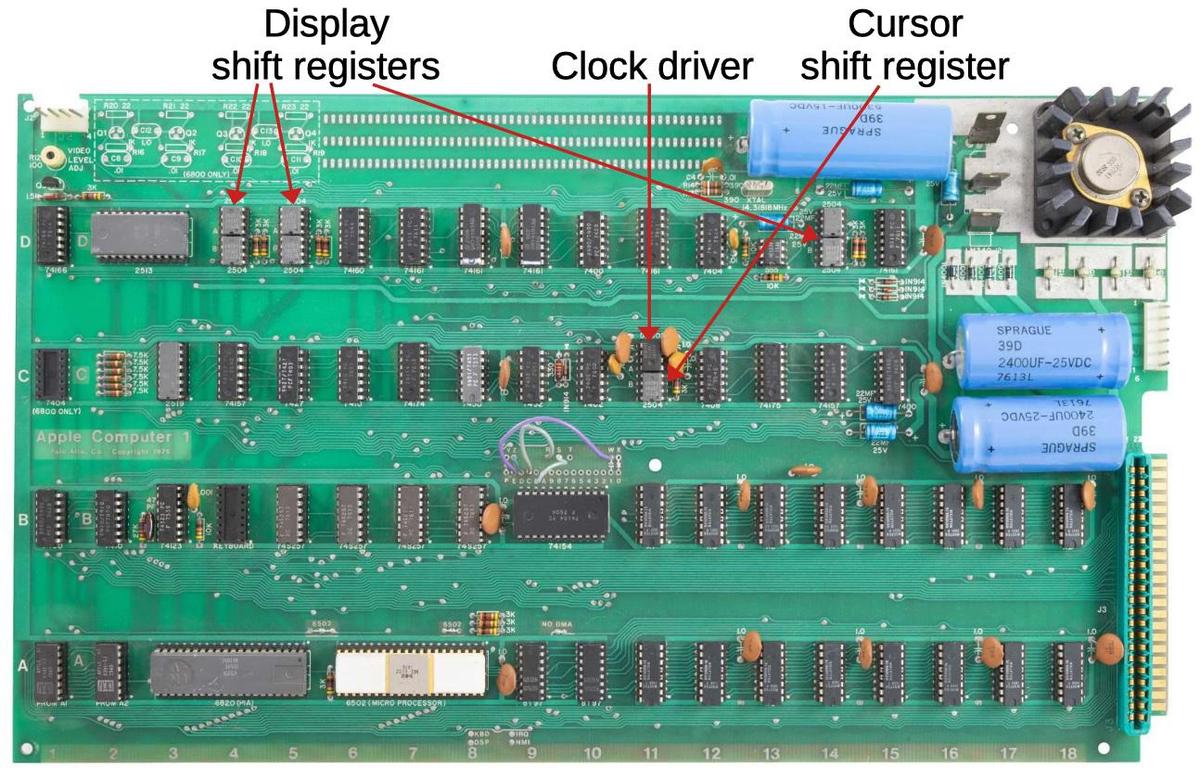
I would love a bit of explanation about why the shift register ICs were spread out so far on the circuit board. Your diagram [1] shows two sets right next to each other with a third set on practically the opposite side of the board. It would almost seem easier to have them all right next to each other so they could cleanly shift. Why the separation?
Oh good, a non-geopolitical question :-) I think there are a few reasons why the shift registers aren't all next to each other. First, there are 6 shift registers (6 bits), but they interact with two 4-bit multiplexers. So you have blocks of three chips to position. Also, the top bit of the shift register is modified for the cursor, so additional chips are required for that shift register. So it's not as easy as putting the shift registers together, since there are other chips involved.
But why are they at opposite sides of the board? I think that is because the shift registers are very simple chips as far as connections, just 6 pins in use. So it is a lot easier to put them at the edges than a chip that has 16 pins in use, since there are only a few lines to route.
Note that the large vertical gap between rows of ICs so there is room for all the horizontal wiring. So I think the board had more capacity for horizontal wiring than vertical wiring. As a result, related circuitry is in the same row. E.g. the display stuff is in the same row (mostly), the CPU, peripheral adapter, and RAM are in the same row, and so forth. I think the video circuitry is in the top row so they can put the output connector at the back.
I'm sure there are more constraints on routing this board that I can only guess at. Even from a quick look, there seem to be a lot of factors.
I saw a photo of this board elsewhere today and I'm also just fascinated by the routing, which seems so completely different from everything else I've seen, even from the era. Were they just trying to make a board where everything, including all traces, components, and connectors, were all on one side? And then they wanted test points on literally every bus line?
Remember, no PCB CAD tools, it was likely laid out by hand - double sized with red/blue tape - the engineer had to work from a (probably) hand drawn schematic and keep all the layout in his head
Hm, fair enough. It's the staggered and widely separated rows that are strange to me.
The photo I saw before was at an angle and I didn't see that some of those spots went 'nowhere'. Looking again at the top down photo/diagram linked above I do see that they're vias now.
First of all, thanks for all your blog posts. It's really interesting to see and understand actual die shots, not just understand it "in theory".
Secondly, how was the shift register actually used? Since every bit pushed in will result in one pushed out, wouldn't that force the input to be pushed in at the same rate as the output and thus the shift register just adds a delay? Or does it happen in two rounds, like so?
1. shift the screen data in and discard output
2. shift the screen data out at a different speed (presumably faster) while shifting in dummy data
Or is there a third option I haven't thought about?
You feed the output of the shift register back into its input. Only when you want to change the display do you break this loop to feed your new character data into it.